High Brightness IPS Displays
Riverdi High Brightness IPS Displays: A New Era of Visual Technology
In the rapidly evolving world of visual technology, Riverdi has consistently stood out as a beacon of innovation and quality. The Riverdi High Brightness IPS Displays series is a testament to our commitment to pushing the boundaries of what’s possible in display technology. These high-resolution, high-brightness TFT displays are equipped with Low-Voltage Differential Signaling (LVDS), or Mobile Industry Processor Interface Display Serial Interface (MIPI DSI) or Red Green Blue (RGB) interfaces, making them a versatile choice for a wide array of applications.


LCD Displays: The Heart of Riverdi’s High Brightness IPS Displays
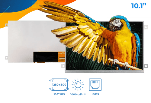
At the core of these innovative displays are LCD monitors, which are renowned for their ability to deliver crisp, clear images. With a typical surface luminance of 1000 cd/m2, these monitors are exceptionally bright, ensuring excellent visibility even in outdoor environments. The high-resolution LCD panels render images with stunning clarity and attention to detail. And the full viewing angles enabled by IPS technology allow for natural, intuitive interaction from any angle.
Whether it’s for an information kiosk, a medical device, or a POS system, these LCD displays are designed to deliver superior visual performance. If you are interested in other Riverdi display solutions, try our Intelligent Displays or the STM32 Display Series.
RGB Displays: Simplicity and Customization
Riverdi’s RGB displays strike an ideal balance between simplicity and customization. The plug-and-play functionality makes these RGB monitors easy to set up and use. But Riverdi also empowers users to tailor these monitors to their specific needs. Options in expanding Riverdi High Brightness RGB monitors include adding a capacitive touchscreen, choosing a metal mounting frame or no frame, and modifying the cover glass. It’s a flexible solution that suits a wide range of applications.
LVDS Displays: High Brightness and Versatility
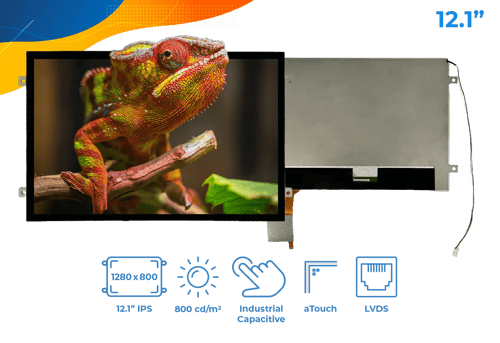
The LVDS displays are designed to offer a high level of brightness, ensuring that they are easily visible even in outdoor settings. They also feature a range of customization options, allowing users to tailor the displays to their specific needs. Whether it’s changing the color, shape, or size of the cover glass, enhancing the brightness of the screen, or choosing a different viewing angle of the display, the LVDS displays offer a level of versatility that is unmatched.
MIPI DSI Displays: The Future of Display Technology
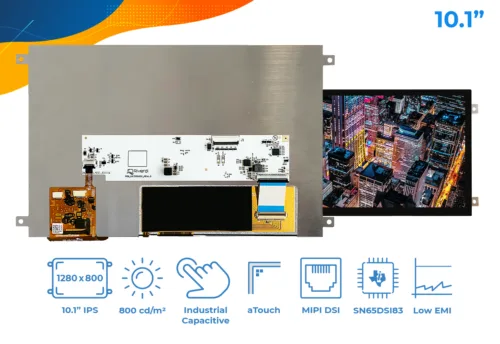
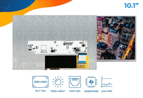
Riverdi’s MIPI DSI displays represent the future of display technology. These displays offer a range of advanced features, including high brightness, full viewing angles, and high resolutions. They are ideal for a variety of applications, including Human Machine Interface (HMI), IoT control, medical devices, laboratory devices, information kiosks, Point of Sale (POS), vending machines, charging stations, and elevator cabins.
Unleashing the Power of Riverdi’s High Brightness IPS Displays
Riverdi’s High Brightness IPS Displays are more than just a visual solution – they are a tool that can transform the way we interact with technology. With their high brightness, full viewing angles, and high resolutions, these displays offer a level of performance that is unmatched.
Applications for Riverdi High Brightness Displays:
- Information kiosks
- Point of sale
- IoT control
- Medical devices
- Laboratory devices
- Vending machines
- Charging stations
- Elevator cabins
- Human Machine Interface (HMI)
High-end technologies in Riverdi High Brightness Displays
Here is some useful information about the high-end technologies we use in our standard products:
Why IPS displays?
The full viewing angles that IPS displays offer will give you the opportunity to see the content clearly from every point of view, unlike TN technology.
Why high brightness displays?
We live in a bright, colorful modern world. It really matters how you present the content on the display. You want the LCD monitors to show all the vibrancy of real life. High-brightness displays have 1000 cd/m2 and allow you to see a clear image even outdoor. High brightness is the key to readability and with Riverdi you have it by standard!
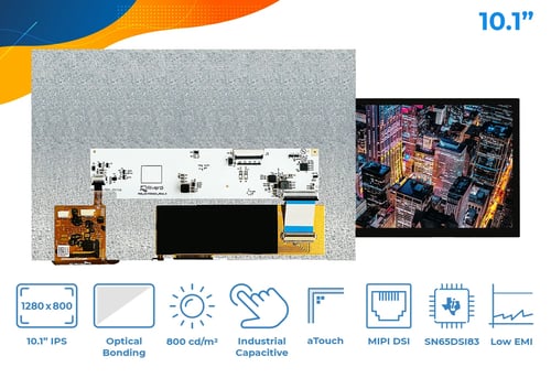
Why Optical bonding?
Optical bonding improves the parameters of the module – the optical performance, as well as durability.
You should choose our high-brightness IPS displays with optical bonding if you want to assure that your display has enhanced optical performance and excellent durability.
Why the industrial CTP controller?
Our skilled engineers are experts in tuning it, so the display can be used with water or gloves. We can easily adapt the touch functionality to every device. Thanks to the CTP controller our displays can pass the highest industrial and medical requirements.
Optical Bonding – Enhancing the optical performance of your display
Optical bonding is a process of affixing the touch panel to the LCD displays using a liquid adhesive, gel or dry film. In general, this process improves the parameters of the module – the optical performance, as well as durability.
When removing the air gaps, we reduce the number of internal reflecting surfaces, which increase of optical performance. This phenomenon improves readability, by reducing the reflection and correct contrast.
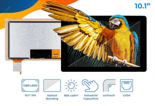
uxTouch
A uxTouch display is a specially designed LCD TFT display which has a Projected Capacitive Touch (PTC). They are the perfect choice for your project if you intend to have an interactive design and technology, thanks to their absolute flat design and multi-touch feature.
Customized LVDS / RGB / MIPI displays
You can customize LCD monitors in many different ways:
- Change the color, shape, and size of the cover glass
- Have your logo printed on the cover glass
- Add a different interface
- Enhance the brightness of the screen
- Change the thickness of the cover lens for the CTP
- Choose a different viewing angle of the display
- Change the pinout
We will help you to get the perfect tailor-made product.